The research conducted within REDFINCH is enabled by a bespoke combination of state-of-the-art facilities, advanced techniques and in-depth expertise available within the consortium.
SiGe Platform
© L. Godart/CEA
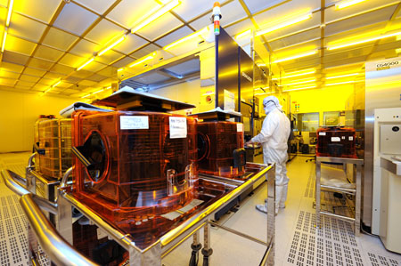
When working in the mid-infrared region, unfortunately standard silicon photonics is no longer the most desirable platform. Although Si itself has excellent transparency at 4.5 μm, the presence of SiO2 leads to strong absorption above about 3.6 μm, severely limiting any practical applications in the MIR wavelength region. Consequently, the REDFINCH project works with a SiGe platform, which can be optimised to provide very low propagation losses across the whole 3–8 μm spectral region. Consortium members have successfully demonstrated a wide range of high-performance passive components (e.g. waveguides, splitters, AWG multiplexers, etc. – see, for example, [1] for details). A comprehensive set of design rules have been established, and the structures can be fabricated within an industry-friendly, pilot line cleanroom environment, ensuring ease of transition to volume production.
- Well-developed SiGe on Si and SiGe on Insulator processes
- Low propagation losses across the whole 3–8 µm region
- PIC structures fabricated in a pilot line environment
III-V on Si Integration Capabilities
For active components such as lasers and detectors, the best performing devices are invariably based on III-V materials. Hence, for a Si-PIC sensor module, it is necessary to combine these III-V devices onto a Si substrate. REDFINCH employs a number of different approaches to achieve this, allowing flexibility to choose the most appropriate method whenever necessary.
Heterogeneous Integration
This is where the III-V device, e.g. a Quantum Cascade Laser (QCL), is grown separately, and then directly bonded onto the Si substrate. It means that the high performance and existing production processes of the III-V devices, developed and optimised over many years, can be directly combined on-chip with the advantages of the SiGe platform for MIR applications. Consortium partners have already successfully demonstrated wafer-level bonding of QCLs on Si, carried out in a Si 200mm production line. Within REDFINCH, this will be extended to optimise the coupling to the low-loss SiGe waveguides, in order to obtain a fully integrated MIR sensor.
Hybrid Integration
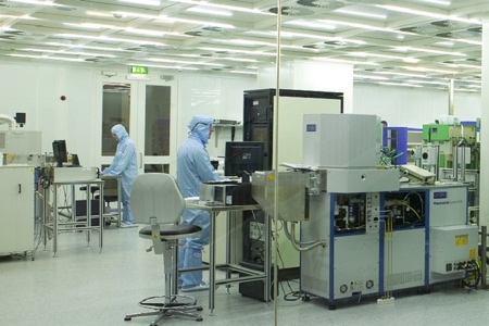
Unlike heterogeneous integration, which is typically performed at the wafer level, hybrid integration combines a variety of processed III-V chips onto a common Si substrate. It is extremely flexible and makes efficient use of materials. Pick and place assembly has been a standard tool in the electronics industry for many years and now provides sub-micron scale precision with high throughput. REDFINCH partners have used eutectic gold-tin solder to bond laser dies to silicon on insulator, with excellent bond strength and very low coupling losses. Since the tolerance to misalignments is proportional to the wavelength, working at the longer MIR wavelengths is an advantage here.
Monolithic Integration
An alternative approach is to grow the III-V device directly on a Si substrate, but this is extremely challenging due to the large lattice mismatch between Si and most III-V semiconductors together with the polar/non-polar interface, which leads to a high density of defects. Moreover, much of the work to date on monolithic integration has focused on the telecoms wavelengths around 1.3 μm and 1.55 μm. However, REDFINCH partners have shown good progress with GaSb-based laser diodes grown on off-axis Si substrates, which can potentially span the whole 1.5–3 μm region, while interband-cascade lasers (ICLs) can extend this to 5 μm. A key focus of REDFINCH will be to investigate the fabrication of localised MIR lasers, i.e. placing them in a specific location on the chip so they are compatible with photonic integrated circuits.
Hybrid Photonic Crystal Lasers
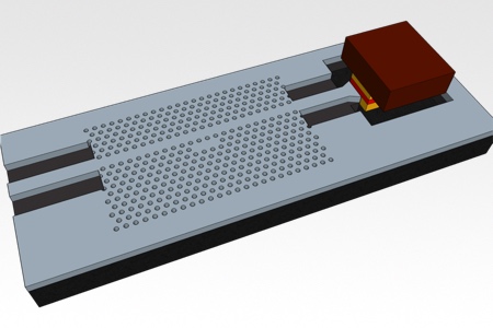
Hybrid lasers, where a III-V gain chip is combined with a Si-based ring resonator, DBR or photonic crystal acting as an external resonant mirror, have recently been demonstrated at the telecoms wavelengths, by REDFINCH partners among others. A photonic crystal is a periodic nanostructure (e.g. formed by holes in a silicon layer) which can present a photonic bandgap in much the same way as a semiconductor lattice forms an electronic bandgap. Since such photonic crystal structures can be arbitrarily constructed using, e.g. e-beam writing, they are a powerful tool for designing and performing a wide range of optical functions. In particular, photonic crystal mirrors can have large Q-factors in the range of 50-100k, allowing the selection of a single longitudinal mode, even though the mirror size is only a few 10s of microns long.
The hybrid arrangement means that the gain and reflector sections can be optimised independently, giving significant cost and performance improvements. For example, a major contributor to low on-wafer yield of MIR DFB lasers is the difficulty in achieving a particular wavelength specification with sufficient power output – both must be achieved simultaneously in the same device in order for it to be viable. However, with the hybrid lasers, the amplifier chip can be chosen based on the power output alone, and paired with a silicon chip screened separately for the desired target wavelength. This increases yields, while also providing lasers with excellent linewidths and low thresholds.